

The onsemi AF0130 and AF0131 intelligent indirect Time-of-Flight (iToF) sensors feature a 1/3.2-inch optical format and backside-illuminated CMOS. They provide global shutter depth and imaging solutions. These sensors come with on-chip functionalities, dual laser driver control, modulation frequencies (up to 200 MHz), and an on-chip laser eye safety threshold.
The AF0130 sensor version is equipped with a depth processing ASIC. It is stacked beneath its pixel area to calculate depth, confidence, and generate intensity maps at high speed from its laser-modulated exposure.
The AF0131 sensor version does not include on-chip depth processing functionality but does offer the same performance. This sensor is suitable for solutions that prefer to perform depth computation outside the chip.
►场景应用图

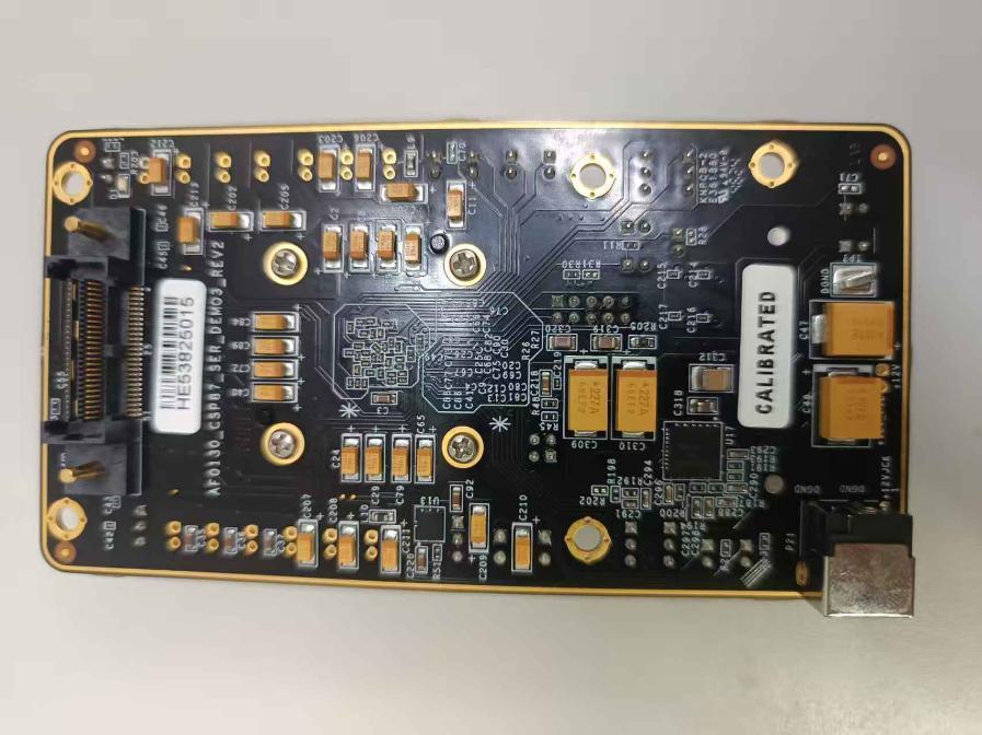
►产品实体图
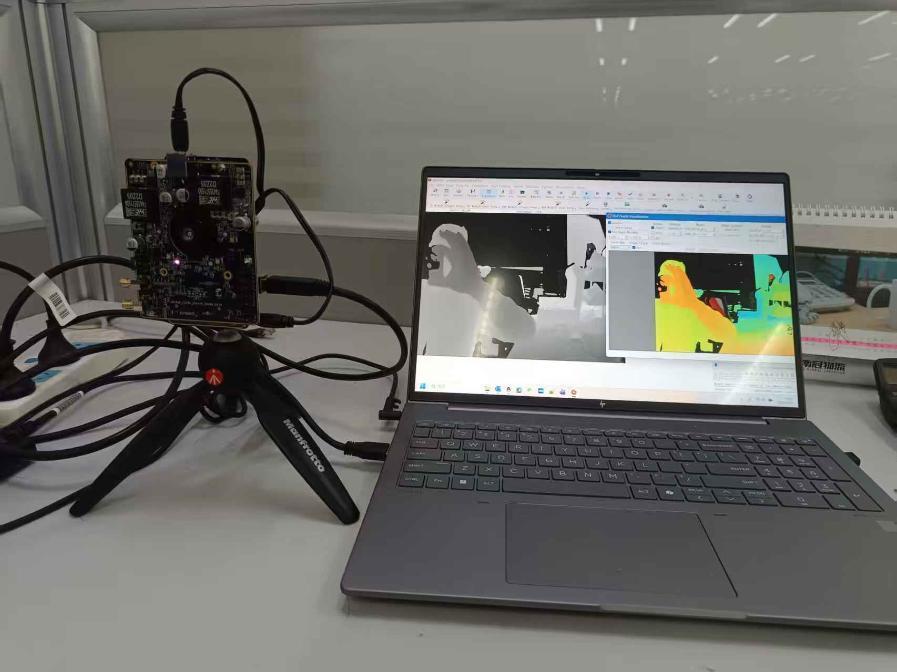
►展示板照片

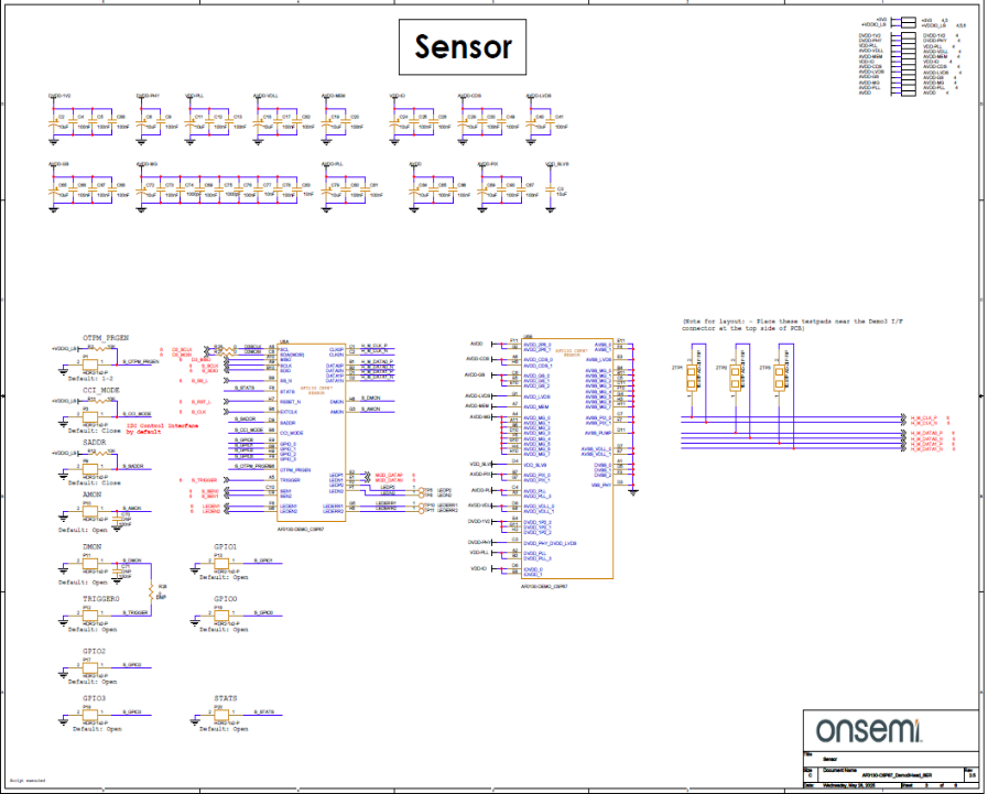
►方案方块图
►核心技术优势
Optical format: 1/3.2 inch (5.60 mm, 4:3 aspect ratio) Effective pixels: 1280 (horizontal) x 960 (vertical) Pixel size: 3.5 x 3.5 µm, back-illuminated (BSI) Chief ray angle: 30° Shutter type: Global shutter One-time programmable memory (OTPM): Three sets of 1024 x 24-bit Input clock range: 10−30 MHz Interface: − Data: MIPI (2 lanes, 2 Gbps per lane) − Host: Two-wire/Four-wire − Laser driver: Three-wire − Laser modulation: LVDS ADC resolution: 10−11 bits Analog gain range: 1−7.75x gain Frame rate: Mode 2.2: Up to 60 fps (1.2 MP), 110 fps (VGA) Mode 3.2: Up to 54 fps (VGA) Read noise: ~6 electrons (with on-chip memory, C1:4) ~3 electrons (from storage gate, SG1:2) Binning: 2x2, 4x4 Maximum signal-to-noise ratio (60°C): Mode 2.2: 46 dB (RAW), 52 dB (intensity) Mode 3.2: 52 dB (RAW), 58 dB (intensity) Dynamic range (60°C): Mode 2.2: 64 dB (RAW), 69 dB (intensity) Mode 3.2: 67 dB (RAW), 72 dB (intensity) Supply voltage: I/O digital: 1.2 V, 1.8 V, 2.8 V Power consumption (Note 1): For 30 fps and 1 ms exposure: ~600 mW (Mode 2.2, 100 MHz) ~900 mW (Mode 3.2, 100+120 MHz) Operating temperature: −30°C < TJ < +85°C Optimal performance temperature: 0°C < TJ < +60°C Package options: − CSP (6.06 x 4.84 mm), 11x8 pins, 0.5 mm pitch − Bare die Thermal resistance: _JA: °C/W (Note 2) 32.0 _JB: °C/W 10.0
►方案规格
1.2 MP CMOS intelligent iToF sensor with advanced 3.5 µm pixel stacked BSI technology Superior low-light and ambient light performance Enhanced near-infrared response (quantum efficiency > 40%) at 850 nm and 940 nm wavelengths Dual-laser (frequency) operation supporting greater depth range (disambiguation) at VGA resolution Low Voltage Differential Signaling (LVDS) driver for modulating two lasers at frequencies up to 200 MHz Two-wire or four-wire serial interface for register access 2 Gbps/channel, 2-channel MIPI CSI-2 D-PHY data interface Laser eye safety monitoring Three output modes: RAW, Data Reduction (DR), Integrated Depth Processing (DP) Supports phase and pulse (hybrid) modulation Simultaneous output of depth, confidence, and grayscale images Horizontal and vertical mirroring, windowing, and pixel binning Equipped with a context state machine with 64 programmable contexts Automatic Exposure Control (AEC) Pixel Defect Identification and Correction (PDI & PDC) Multi-camera and interference mitigation features Reduced motion artifacts due to decoupling of integration and readout Hardware trigger control On-chip averaging and histogram statistics for intelligent control On-chip temperature sensor These devices are compliant with lead-free and RoHS standards