

onsemi's High-Voltage Switcher is a power component that integrates a PWM controller and a high-voltage MOSFET into a single package. The PWM controller is typically a fixed switching frequency flyback converter or a variable frequency quasi-resonant flyback converter (QR flyback) controller. The high-voltage MOSFET generally operates with voltages ranging from 600V to 1000V, with an RDS(ON) typically between 1 ohm and 10 ohms. High-voltage switchers are commonly available in DIP and SMD packages. Common DIP packages include DIP-8 and DIP-7 (as shown in Figure 1), while SMD packages include SIOC-8, SIOC-7, SOT-223 (as shown in Figure 2), or TO-89, among others. Due to limitations in packaging or thermal conditions, the output power of high-voltage switchers is typically below 50 watts. As a result, high-voltage switchers are often used in auxiliary power supplies or standby power supplies. Common application scenarios include auxiliary power for white goods, smart meters, and industrial power supplies.

Figure 1, DIP-7 package

Figure 2, SOT-223 package
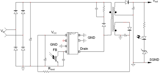
Today, we are introducing the star of the show, the onsemi NCP107x series high-voltage switcher. It is a fixed-frequency current-mode controller that integrates a 700V MOSFET within the same package. This product is suitable for applications with an input voltage range of 90Vac to 264Vac. Figure 3 shows a typical application circuit of the NCP107x, which is very simple and ideal for auxiliary power supplies. Additionally, the onsemi NCP107x series high-voltage switcher features a dynamic self-high-voltage startup function, allowing the controller to start easily without the need for an additional auxiliary power supply. The NCP107x series high-voltage switcher also provides a 1ms soft start function to reduce stress during startup and effectively minimize output overshoot issues. Furthermore, the NCP107x series high-voltage switcher includes a frequency jittering function, which helps disperse energy around the main switching components, thereby achieving EMI softening effects. The Flyback application circuit of the onsemi NCP107x series high-voltage switcher is also very simple, as shown in Figure 3, and it offers a comprehensive set of features.
1. Output Short Circuit Protection: Utilizes an auto-recovery protection mechanism with timer-based detection.
2. Over Voltage Protection: Automatic recovery protection mechanism for over voltage protection implemented through auxiliary winding.
3. Frequency Jittering and Frequency Foldback Mode functions: These are used to spread the EMI energy of the main switching components and to limit the range of switching frequency to optimize EMI performance. Additionally, the Frequency Foldback Mode function can also optimize efficiency under light load conditions.
4. Internal Temperature Shutdown protection.

Figure 3: Typical application circuit diagram of the NCP107x series
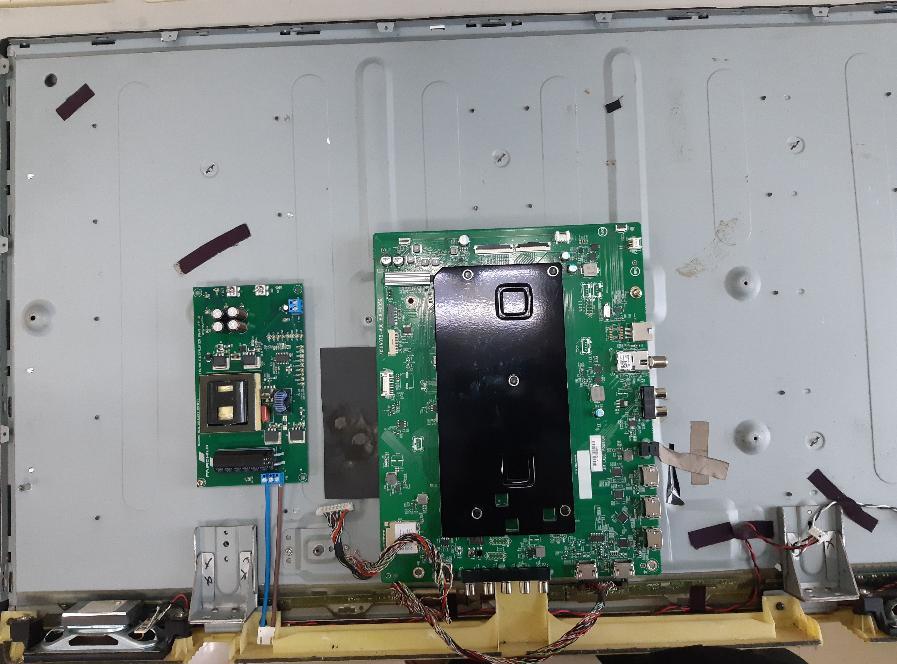
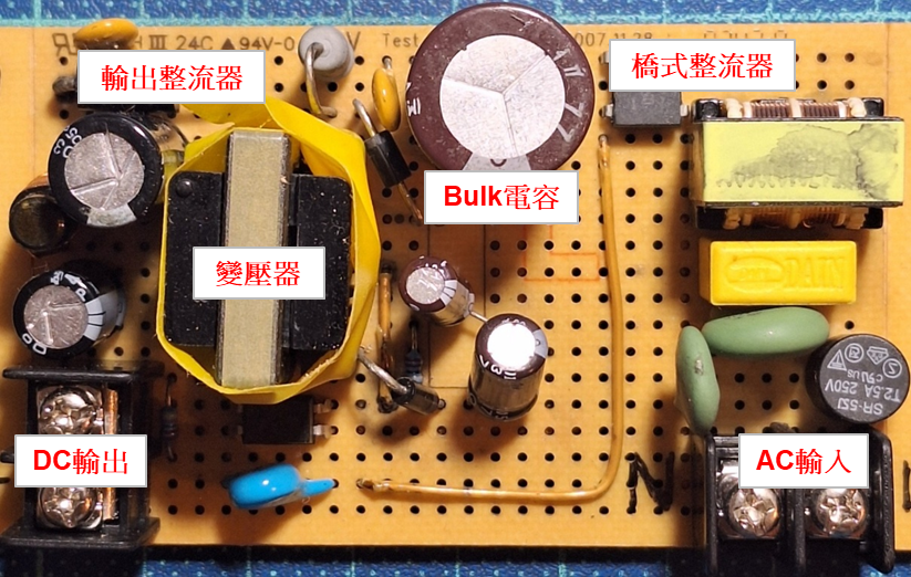
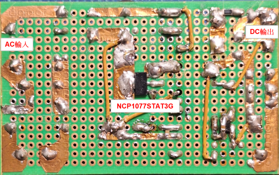
Today's topic focuses on the application of the ON Semiconductor NCP1077STAT3G as a 12V/12W auxiliary power supply. The main specifications are as follows: input voltage range is 90Vac~264Vac, full load efficiency is greater than 75%, and output voltage variation must be controlled within 3%. The circuit diagram is designed based on the typical application circuit shown in Figure 3, using an EE22 transformer core. According to the BCM formula, the primary inductance of this 12V/12W transformer can be calculated, and we use an inductance value of 1mH. The primary-to-secondary turns ratio is 6:1, specifically NP:NS:NVCC = 74Ts : 12Ts : 12Ts. The solution uses a 100V/3A Schottky diode as the secondary side output rectifier. The 12V/12W auxiliary power supply solution is assembled using readily available components, and the PCB is implemented on a prototyping board. The finished product after assembly is shown in Figure 4. The full load efficiency of the 12V/12W auxiliary power supply solution is 77.97% at 90Vac, 79.63% at 115Vac, 78.84% at 230Vac, and 77.77% at 264Vac. Figure 5 shows the efficiency performance of the 12V/12W auxiliary power supply solution under different input voltages and loads. The no-load power consumption of the 12V/12W auxiliary power supply solution is 107mW at 90Vac, 152mW at 115Vac, 570mW at 230Vac, and 752mW at 264Vac. Figure 6 shows the no-load power consumption performance under different input voltages. The output voltage variation is a maximum of 0.33% at 90Vac, 0.33% at 115Vac, 0.33% at 230Vac, and 0.33% at 264Vac. Figure 7 shows the output voltage variation under different input voltages and loads. The output voltage rise time of the 12V/12W auxiliary power supply solution is 17.6ms at 90Vac and 11.4ms at 264Vac. Figure 8 shows the output voltage rise time at 90Vac, and Figure 9 shows the output voltage rise time at 264Vac. The maximum voltage stress of NCP1077 VDS under full load is 330V at 90Vac and 558V at 264Vac. Figure 10 shows the VDS voltage waveform at 90Vac full load, and Figure 11 shows the VDS voltage waveform at 264Vac full load. The maximum voltage stress of the secondary side rectifying Schottky diode is 43.2V at 90Vac and 86.4V at 264Vac. Figure 12 shows the voltage waveform of the secondary side rectifying Schottky diode at 90Vac full load, and Figure 13 shows the voltage waveform at 264Vac full load.
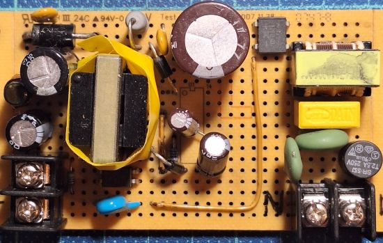
Figure 4: Actual 12W/12V finished product
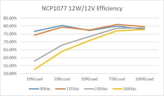
Figure 5: Efficiency under various input voltages and loads
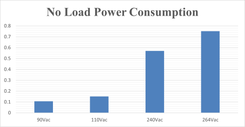
Figure 6: No-load power consumption performance under various input voltages
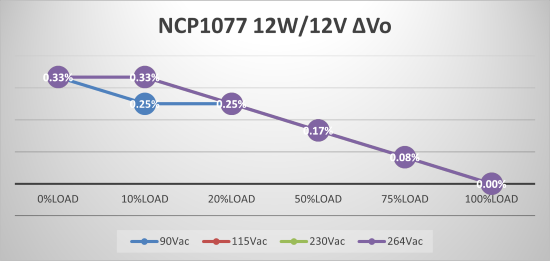
Figure 7: Output voltage variation rate under various input voltages and loads
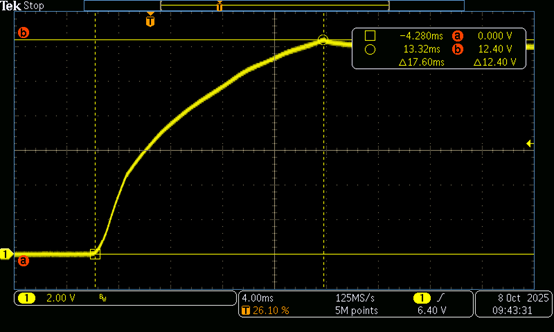
Figure 8: 12Vo output rise time at 90Vac
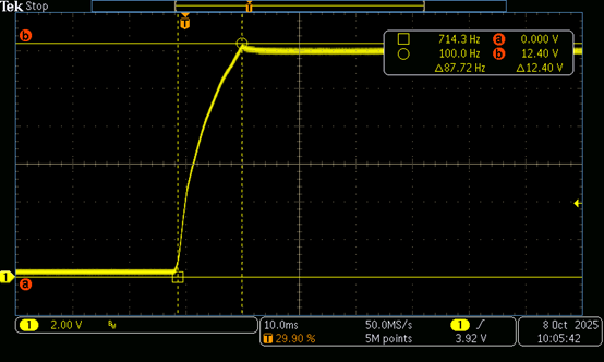
Figure 9: 12Vo rise time at 264Vac
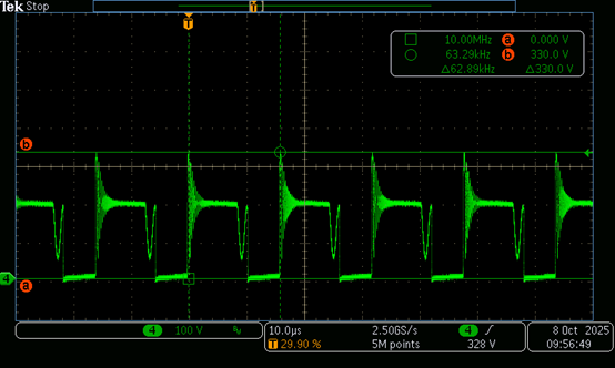
Figure 10: Voltage stress waveform of NCP1077 at full load with 90Vac
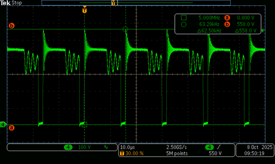
Figure 11: Voltage stress waveform of NCP1077 under full load at 264Vac
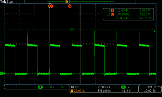
Figure 12: Output rectifier diode voltage stress waveform at full load with 90Vac input.
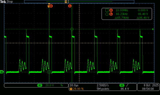
Figure 13: Output rectifier diode voltage stress waveform at 264Vac full load.
►场景应用图
►展示板照片
►方案方块图
►核心技术优势
1. Fixed frequency operation 2. Provides internal soft start 3. Offers frequency jittering function 4. Short-circuit protection function 5. Dynamic Self-Supply (DSS) function 6. Skip-cycle function 7. Maximum peak current setting 8. Includes internal slope compensation
►方案规格
1. Input Voltage: 90Vac ~ 264Vac 2. Output Voltage: 12Vdc 3. Output Voltage Accuracy: +/- 1% 4. Maximum Output Current: 1A 5. Efficiency: 75% (Output Voltage=12V; Output Current=1A) 6. Output Voltage Rise Time: less than 20ms 7. Demo Board PCB Dimensions (LxWxH): 80 mm x 50 mm x 25 mm