

Onsemi's High-Voltage Switcher is a power device that integrates a PWM controller with a high-voltage MOSFET in a single package. The PWM controller is typically a fixed switching frequency flyback converter or a variable frequency quasi-resonant flyback converter (QR flyback) controller. The high-voltage MOSFET generally operates with voltages ranging from 600V to 1000V, with an RDS(ON) range between 1 ohm and 10 ohms. High-voltage switchers are commonly packaged in DIP and SMD formats, with typical DIP packages including DIP-8 and DIP-7 (as shown in Figure 1), and SMD packages such as SIOC-8, SIOC-7, SOT-223 (as shown in Figure 2), or TO-89. Due to limitations in packaging or thermal conditions, the output power of high-voltage switchers is usually below 50 watts, making them suitable for auxiliary power or standby power applications. Common use cases include auxiliary power for white goods, smart meters, and industrial power supplies.

Figure 1, DIP-7 package

Figure 2, SOT-223 package
Today, we are introducing the main feature of the ON Semiconductor NCP107x series high-voltage switcher. It is a fixed-frequency current-mode controller that integrates a 700V MOSFET within the same package. This product is suitable for applications with an input voltage range of 90Vac to 264Vac. Figure 3 shows a typical application circuit of the NCP107x, which has a very simple circuit design, making it ideal for auxiliary power supplies. Additionally, the ON Semiconductor NCP107x series high-voltage switcher offers dynamic self-high-voltage startup functionality, allowing the controller to start easily without requiring an additional auxiliary power supply. The NCP107x series high-voltage switcher also provides a 1ms soft start function to reduce stress during startup and effectively minimize output overshoot issues. Furthermore, the NCP107x series high-voltage switcher features a frequency jittering function, which helps disperse the energy around the main switching components, thereby achieving EMI reduction. The Flyback application circuit of the ON Semiconductor NCP107x series high-voltage switcher is also very simple, as shown in Figure 3, and it offers a variety of comprehensive features.
1. Output Short Circuit Protection: Utilizes an auto-recovery protection mechanism with timer-based detection.
2. Over Voltage Protection: An automatic recovery protection mechanism for over voltage protection achieved through auxiliary windings.
3. Frequency Jittering and Frequency Foldback Mode: These are used to spread the EMI energy of the main switching components and limit the switching frequency range to optimize EMI performance. Additionally, the Frequency Foldback Mode function can also optimize efficiency performance under light load conditions.
4. Internal Temperature Shutdown protection.
In summary, the ON Semiconductor NCP107x series high-voltage switcher is a well-rounded, simple yet efficient solution suitable for various application scenarios.
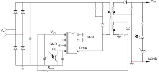
Figure 3: Typical Application Circuit Diagram of the NCP107x Series
Today's topic focuses on the application of the onsemi NCP1077STAT3G for a 12V/12W auxiliary power supply. The main specifications are as follows: input voltage range is 90Vac~264Vac, full-load efficiency is greater than 75%, and output voltage variation must be controlled within 3%. The circuit diagram is designed based on the typical application circuit shown in Figure 3, using an EE22 core transformer. According to the BCM formula, the primary inductance of this 12V/12W transformer can be calculated, and here we use an inductance value of 1mH with a primary-to-secondary turns ratio of 6:1. This 12V/12W auxiliary power supply is assembled using readily available components, and the PCB is implemented on a prototyping board. The actual assembled product is shown in Figure 4. The actual full-load efficiency of the board is 77.97% at 90Vac, 79.63% at 115Vac, 78.84% at 230Vac, and 77.77% at 264Vac. Figure 5 shows the efficiency of this product under different input voltage and load conditions. The output voltage variation is a maximum of 0.33% at 90Vac, 0.33% at 115Vac, 0.33% at 230Vac, and 0.33% at 264Vac. Figure 6 illustrates the output voltage variation of this product under different input voltage and load conditions.
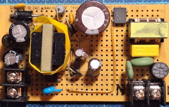
Figure 4: Actual 12W/12V Finished Product
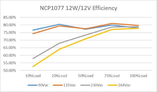
Figure 5: Efficiency under various input voltages and loads
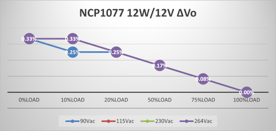
Figure 6: Output voltage variation rate under different input voltages and loads