

NXP MC33771 與外部通訊的介面分為 SPI interface and TPL interface. 此處先介紹 TPL interface communication.
TPL ( transceiver physical layer transformer ),最高速率可以達到 2.0Mbps. 透過差動訊號來降低傳輸上錯誤發生。
由於多數的 MCU 沒有包含 TPL 的驅動,因此會透過 NXP MC33664 把 SPI 轉為 TPL 訊號跟 MC33771 通訊。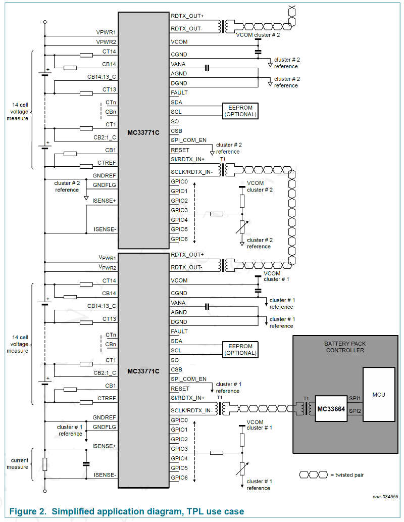
MC33664 是一個透過 SPI interface 把訊號轉換成 TPL 的 transceiver.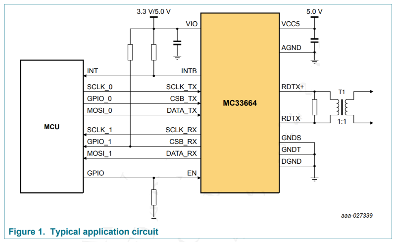
包含兩組 SPI interface 用來做資料的確認。
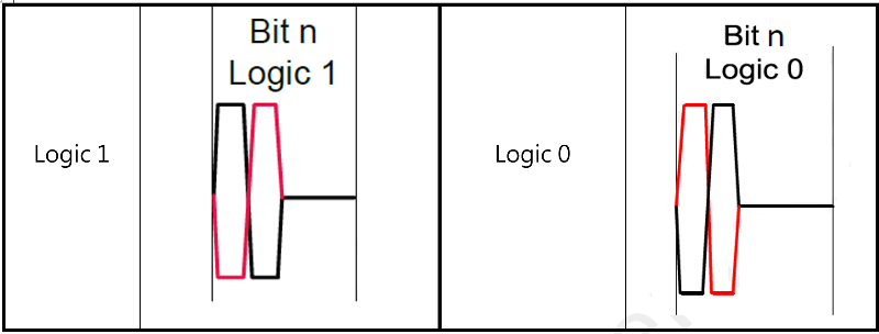
TPL 是透過雙絞線的脈衝來轉為 Logic 0 or 1. 總共可以分為三種脈衝的型態如圖 2.1 分為 positive, negative, and zero.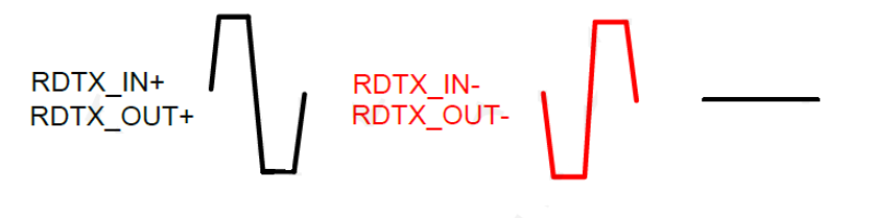
每次封包的一開始會發出一個起始訊號,稱為 SOM ( Start – of – message ),結束需要一個終止訊號 EOM ( End – of – message ).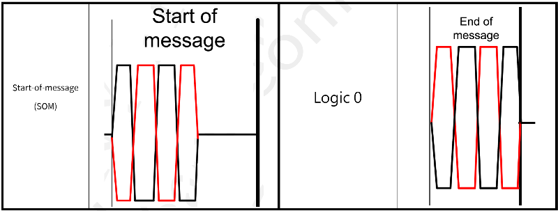
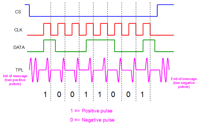
一段封包的長度固定為 48 bits. 通訊結構類似於 SPI interface. TPL 傳輸會透過 Daisy chain 進行多級串接,在初始化後,會先對第一級的 device 進行 CID 編成,給定號碼後進再透過第一級向第二級給 CID,以此類推…此處的 CID 由 6 bits 決定,因此可以定義1~63個。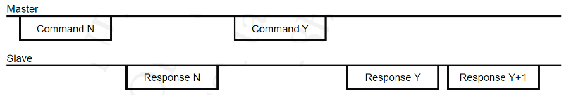
如果 MC33771 收到錯誤或不完整的封包,MC33771 會傳出 error 的 Flag. 直到收到完整的封包才會進一步地回應。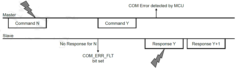
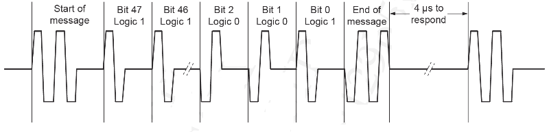
在每段封包之間需要有 4us 的 respond time。
六、SPI Introduction介紹 SPI ( Serial Peripheral Interface),最高速率可以達到 4.0Mbps.
七、SPI communication
NXP MC33771 SPI interface 操作電壓落在 5.0V 但同樣也可以接受 3.3V 訊號,但需要再 MISO pin 串接 5.23k ohm. 因為 MC33771 內部 MISO driver 為 5.0V需要進行衰減。
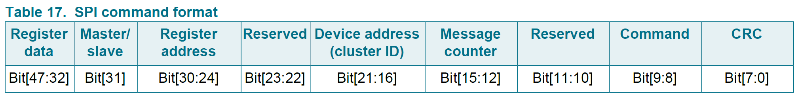
SPI 傳輸的封包長度為 48-bit. 其內容分為
- Register data (16 bits).
- Master/slave (1 bit), always at 1 in the response.
- Register address (7 bits).
- Reserved (2 bits).
- Cluster ID (6 bits).
- Message counter (4 bits).
- Reserved (2 bits).
- Command (2 bits).
- Cyclic redundancy check (8 bits)
在初始化通訊後,MCU 會將 CSB 由高電平轉為低電平。MSB 傳輸, MOSI data 在 falling edge 的 SCLK. MISO 資料在 rising edge 被讀取。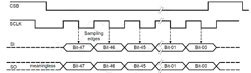
下圖為 SPI 傳輸過程的一段封包,前面屬於我們所下達的 command, MC33771 回傳回來的 response .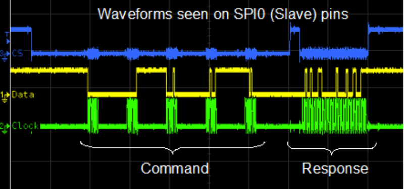
|
Register address |
symbol |
Description |
|
0x01 |
INIT |
Device initialization |
|
0x02 |
SYS_CFG_GLOBAL |
Global system configuration |
|
0x03 |
SYS_CFG1 |
System configuration |
|
0x04 |
SYS_CFG2 |
System configuration |
|
0x05 |
SYS_DIAG |
System diagnostic |
|
0x06 |
ADC_CFG |
ADC configuration |
|
0x07 |
ADC2_OFFSET_ COMP |
ADC2 offset compensation |
|
0x08 |
OV_UV_EN |
CT measurement selection |
|
0x09 |
CELL_OV_FLT |
CT overvoltage fault |
|
0x0A |
CELL_UV_FLT |
CT undervoltage fault |
|
0x0B |
TPL_CFG |
TPL configuration for up and down Transmitter |
|
0x0C~0x19 |
CBx_CFG |
CB configuration for cell x |
|
0x1A |
CB_OPEN_FLT |
Open CB fault |
|
0x1B |
CB_SHORT_FLT |
Short CB fault |
|
0x1C |
CB_DRV_STS |
CB driver status |
|
0x1D |
GPIO_CFG1 |
GPIO configuration |
|
0x1E |
GPIO_CFG2 |
GPIO configuration |
|
0x1F |
GPIO_STS |
GPIO diagnostic |
|
0x20 |
AN_OT_UT_FLT |
AN over and undertemperature |
|
0x21 |
GPIO_SHORT_ ANx_OPEN_STS |
Short GPIO/open AN diagnostic |
|
0x22 |
I_STATUS |
PGA DAC value |
|
0x23 |
COM_STATUS |
Number of CRC error counted |
|
0x24~0x26 |
FAULTx_STATUS |
Fault status |
|
0x27~0x29 |
FAULT_MASKx |
FAULT pin mask |
|
0x2A~0x2C |
WAKEUP_MASK x |
Wake-up events mask |
|
0x2D |
CC_NB_SAMPLES |
Number of samples in coulomb counter |
|
0x2E~0x2F |
COULOMB_CNTx |
Coulomb counting accumulator |
|
0x30~0x31 |
MEAS_ISENSEx |
ISENSE measurement |
|
0x32 |
MEAS_STACK |
Stack voltage measurement |
|
0x33~0x40 |
MEAS_CELL x |
Cell x voltage measurement |
|
0x41~0x47 |
MEAS_ANx |
ANx voltage measurement |
|
0x48 |
MEAS_IC_TEMP |
IC temperature measurement |
|
0x49 |
MEAS_ VBG_DIAG_ADC1A |
ADCIA voltage reference measurement |
|
0x4A |
MEAS_ VBG_DIAG_ADC1B |
ADCIB voltage reference measurement |
|
0x4B |
TH_ALL_CT |
CTx over and undervoltage threshold |
十、Reference 參考資料
- MC33664 Datasheet https://www.nxp.com/docs/en/data-sheet/MC33664_SDS.pdf
- MC33771 Datasheet https://www.nxp.com/docs/en/data-sheet/MC33771B_SDS.pdf