

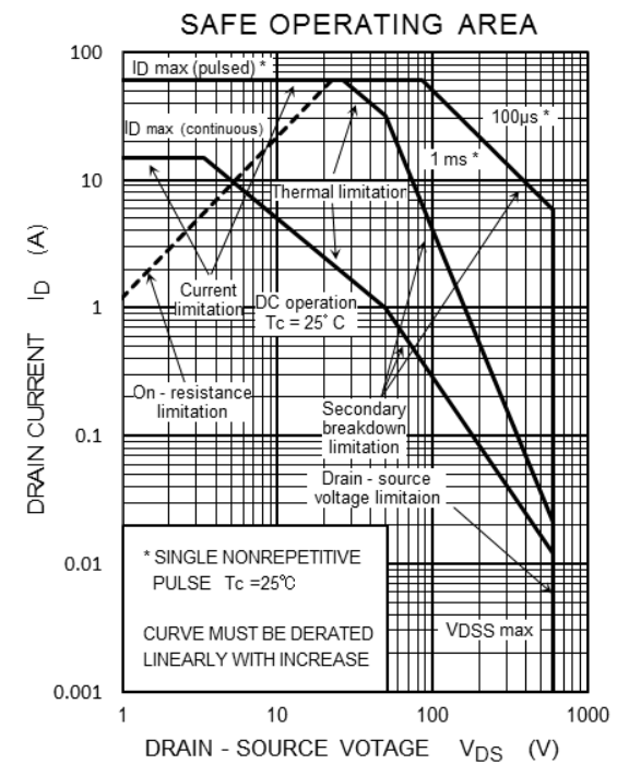
本篇將介紹 TOSHIBA MOSFET 的 MOSFET SOA的 Temperature derating.如圖一所示,
圖一:MOSFET SOA(註一:Derating of the MOSFET Safe Operating Area)
這裡我們舉一個例子說明,當Tc= 100°C 計算如下, 圖二顯示, 當MOSFET 的 PD – Tc 特性,PD(Tc = 100°C) 可以使用公式1.進行計算,PD(Tc = 100°C) 計算為 20 W
如下圖所示,請注意,公式1. 適用於受熱限制限制的區域.
公示1.(註一:Derating of the MOSFET Safe Operating Area)
圖二: PD-Tc特性曲線(註一:Derating of the MOSFET Safe Operating Area)
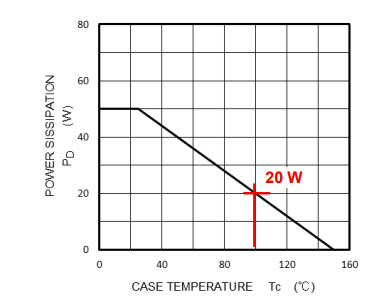
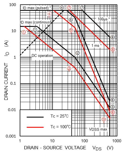
接下來我們將介紹TC =25°C時的 SOA 曲線介紹,如圖三所示, ① 和 ② 處於熱限制範圍內, ①和②在PD 的等功率線(最大)= 50 W(VDS × ID = 50 W). 當 Tc = 100°C 時的功耗如圖二所示的 20W 等功率線.
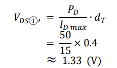
①' 和 ②' 可使用公式3.和公式4,計算,方法是使用公式2. 將 ① 處的 VDS 和 ② 處的 ID Derating至 40%
公式2.(註一:Derating of the MOSFET Safe Operating Area)
公式3.(註一:Derating of the MOSFET Safe Operating Area)
公式4.(註一:Derating of the MOSFET Safe Operating Area)
圖三: MOSFET SOA 的Temperature derating曲線(註一:Derating of the MOSFET Safe Operating Area)
圖一:MOSFET SOA(註一:Derating of the MOSFET Safe Operating Area)
這裡我們舉一個例子說明,當Tc= 100°C 計算如下, 圖二顯示, 當MOSFET 的 PD – Tc 特性,PD(Tc = 100°C) 可以使用公式1.進行計算,PD(Tc = 100°C) 計算為 20 W
如下圖所示,請注意,公式1. 適用於受熱限制限制的區域.
公示1.(註一:Derating of the MOSFET Safe Operating Area)
圖二: PD-Tc特性曲線(註一:Derating of the MOSFET Safe Operating Area)
接下來我們將介紹TC =25°C時的 SOA 曲線介紹,如圖三所示, ① 和 ② 處於熱限制範圍內, ①和②在PD 的等功率線(最大)= 50 W(VDS × ID = 50 W). 當 Tc = 100°C 時的功耗如圖二所示的 20W 等功率線.
①' 和 ②' 可使用公式3.和公式4,計算,方法是使用公式2. 將 ① 處的 VDS 和 ② 處的 ID Derating至 40%
公式2.(註一:Derating of the MOSFET Safe Operating Area)
公式3.(註一:Derating of the MOSFET Safe Operating Area)
公式4.(註一:Derating of the MOSFET Safe Operating Area)
圖三: MOSFET SOA 的Temperature derating曲線(註一:Derating of the MOSFET Safe Operating Area)
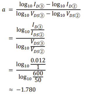
通過②的直線的斜率a 和 ③ 可以藉由公式5.計算如下:
公式5.(註一:Derating of the MOSFET Safe Operating Area)
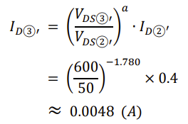
Derating後,線路經過②’,斜率為a.因此,③’處的ID可以使用公式 6. 計算如下:
公式6.(註一:Derating of the MOSFET Safe Operating Area)
接著我們將繼續介紹 Derating 在 tw = 1 ms 曲線.
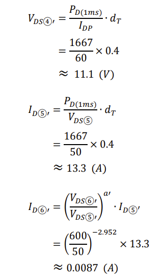
tw = 1 ms,PD(1 ms) 時的功耗根據以下公式計算約為 1667 W:瞬態熱阻抗曲線如圖四所示. Derating通過的點
Tc = 100°C 時的熱限制線(④' 至 ⑤')和二次擊穿限制( ⑤' 至 ⑥' ) 通過的計算方法與 Tc = 25°C(DC 操作)線相同.
圖四: 熱阻抗曲線(註一:Derating of the MOSFET Safe Operating Area)
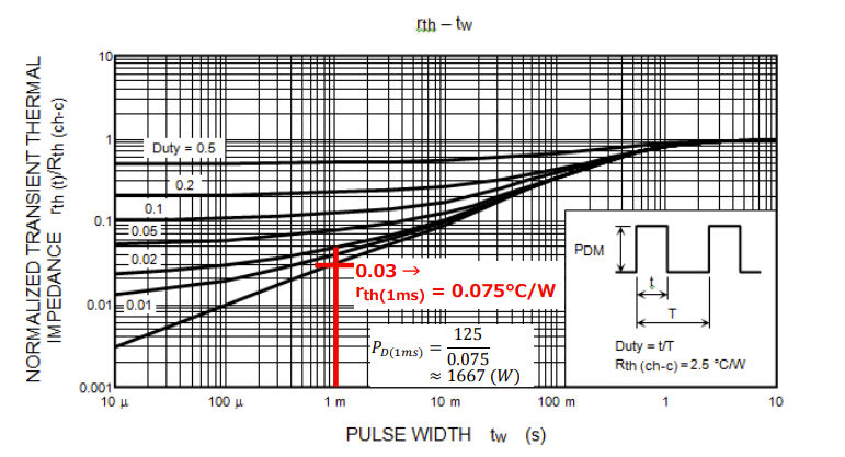
公式7.~公式8.(註一:Derating of the MOSFET Safe Operating Area)
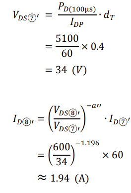
最後我們將介紹Derating在 tw = 100 μs 曲線,這條線的斜率 (a'' ) 經計算約為 -1.196,位於熱力限制範圍之外. VDS⑦’和 ID⑧’可以分別使用公式9.和公式10. 計算:公式9.~公式10.(註一:Derating of the MOSFET Safe Operating Area)
以上就是TOSHIBA MOSFET SOA曲線的介紹提供給各位參考.